 ESPCI web site



Neuromorphic
Contact:  " class="spip_mail">Alexandre ZIMMERS
Quantum materials for brain-inspired computing
Introduction · Optical imaging · Memory effects · Local control · Publications · Video
Towards brain-inspired computing
The brain-inspired algorithms of the AI revolution primarily run on conventional silicon-based computer architectures that were not designed for this purpose. As artificial intelligence continues to grow, its energy demands are becoming an increasingly important challenge.
Neuromorphic computing offers a promising alternative by mimicking the brain’s basic components—neurons and synapses—ideally using a single material.
Among the few quantum materials capable of naturally producing neuron-like electrical spikes, vanadium dioxide (VO₂) stands out as a promising candidate for artificial neurons, known as neuristors. However, implementing reliable, rewritable synaptic memory—synaptors—in the same material remains a key challenge.

Fig. 1. Schematic illustration of a neuromorphic system. (a) Biological model: the neuron soma receives inputs via synapses. (b) Bio-inspired electronic model: an electronic neuristor accumulates inputs generated by multiple pre-synaptic neuristors, with weights modulated by memristive synaptors. Bottom: VO₂ naturally functions as an artificial neuron, while its potential as an artificial synapse is being explored.
Visualizing electronic patterns in VO₂
Vanadium dioxide undergoes a remarkable insulator–metal transition near 68 °C, accompanied by a dramatic change in electrical resistance.
To understand and eventually control this transition, we first investigated its spatial organization. The transition gives rise to complex electronic patterns, with metallic and insulating domains displaying fractal structures over multiple length scales.
We developed a new optical microscopy method that enables sub-micron imaging of these patterns. By following their evolution during temperature cycles, we reconstructed local transition-temperature and hysteresis maps (1) and revealed underlying interactions using machine-learning techniques (2).
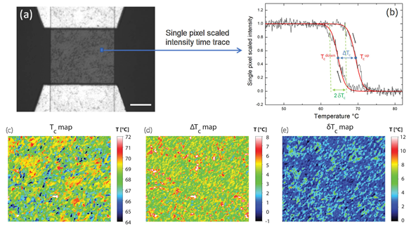
Fig. 2. Multiscale electronic patterns in VO₂ during the insulator–metal transition.
Read the publication — Condensed Matter (2025)
From microscopic images to electrical resistance
More recently, we established a quantitative link between microscopic electronic patterns and macroscopic electrical transport in VO₂.
By incorporating the fractal structure of electronic domains into a multiscale resistor-network model, we can accurately predict macroscopic resistance from optical microscopy images across the insulator–metal transition (7).
Read the new study — arXiv (2025)
Engineering memory in VO₂
A crucial step towards single-material neuromorphic computing is to introduce synaptic memory into VO₂.
We have demonstrated a remarkable memory phenomenon known as Ramp Reversal Memory (RRM). By partially cycling the temperature through the insulator–metal transition, the resistance can be modified in a history-dependent manner.
Using spatially resolved optical imaging, we showed that this memory is encoded throughout the material, rather than being confined to isolated regions (3).
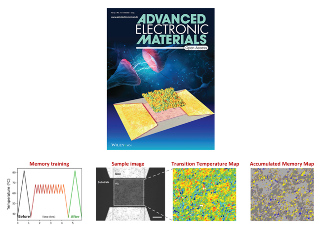
Fig. 3. Spatially Distributed Ramp Reversal Memory in VO₂.
Read the publication — Advanced Electronic Materials (2023)
Understanding the role of interactions
More recently, we demonstrated that interactions between metallic and insulating domains play an important role in Ramp Reversal Memory.
By combining a correlated Random Field Ising Model with defect diffusion and segregation, we developed a theoretical framework to explain how domain interactions influence and enhance the memory effect (6).
These results provide new insights into the physical mechanisms governing memory in phase-separated quantum materials.
Read the new publication — Advanced Electronic Materials (2025)
Local control and optical programming
Beyond temperature-induced memory, we have developed methods for controlling the insulator–metal transition locally.
Using a focused laser beam, we demonstrated that it is possible to create microscopic metallic patterns within an insulating VO₂ junction, thereby tuning its electrical resistance on demand.
These patterns can persist while the temperature is maintained within the hysteresis region. They can be erased by lowering the temperature or partially modified using an atomic force microscope (AFM) tip (4).
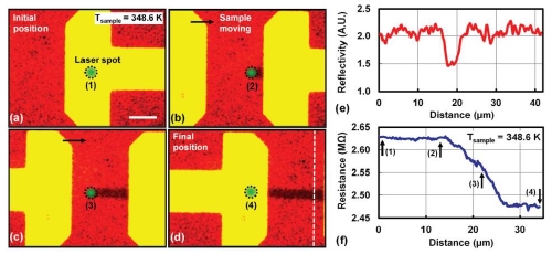
Fig. 4. Local control of VO₂ insulator–metal patterns using temperature sweeps, a focused laser beam, and an AFM tip.
Read the publication — Advanced Electronic Materials (2025)
Plasmon-assisted control
We have also explored the use of gold nanostructures to locally modify the transition conditions of VO₂.
Ordered arrays of Au nanodisks enhance the photothermal response, reducing the laser power required to induce the insulator–metal transition and providing an additional means of controlling the material’s electronic state (5).
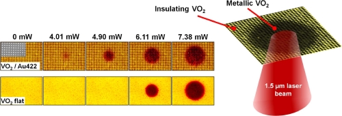
Fig. 5. Plasmon-enhanced photothermal control of the insulator–metal transition in VO₂ using ordered arrays of gold nanodisks.
Read the publication — Surfaces and Interfaces (2025)
Towards single-material neuromorphic architectures
Together, these advances open the possibility of creating programmable and rewritable synaptic connections between neuristors in a single-material VO₂ neuromorphic chip.
By combining microscopic imaging, a deeper understanding of domain interactions, and local optical control, we aim to develop new approaches to energy-efficient neuromorphic computing.
Selected publications
[1] Optical Mapping and On-Demand Selection of Local Hysteresis Properties in VO₂
M. Alzate Banguero, S. Basak, N. Raymond, F. Simmons, P. Salev, I. K. Schuller, L. Aigouy, E. W. Carlson, A. Zimmers.
Condensed Matter 10 (1), 12 (2025).
[2] Deep learning Hamiltonians from disordered image data in quantum materials
S. Basak, M. A. Banguero, L. Burzawa, F. Simmons, P. Salev, L. Aigouy, M. M. Qazilbash, I. K. Schuller, D. N. Basov, A. Zimmers, E. W. Carlson.
Physical Review B 107, 205121 (2023).
[3] Spatially Distributed Ramp Reversal Memory in VO₂
S. Basak, Y. Sun, M. A. Banguero, P. Salev, I. K. Schuller, L. Aigouy, E. W. Carlson, A. Zimmers.
Advanced Electronic Materials 9 (10), 2300085 (2023).
[4] Tuning the Resistance of a VO₂ Junction by Focused Laser Beam and Atomic Force Microscopy
Z. Fang, M. Alzate-Banguero, A. R. Rajapurohita, F. Simmons, E. W. Carlson, Z. Chen, L. Aigouy, A. Zimmers.
Advanced Electronic Materials 11 (2), 2400249 (2025).
[5] Plasmon-enhanced photothermal sensing through coupled VO₂/Au nanodisks
Z. Fang, A. Zimmers, Z. Chen, L. Billot, A. García-Martín, L. Aigouy.
Surfaces and Interfaces 62, 106145 (2025).
[6] Interactions Enhance Ramp Reversal Memory in Locally Phase Separated Materials
Y. Sun, M. Alzate Banguero, P. Salev, I. K. Schuller, L. Aigouy, A. Zimmers, E. W. Carlson.
Advanced Electronic Materials 11 (21), e00489 (2025).
[7] Accurate prediction of macroscopic transport from microscopic imaging via critical fractals at the Mott transition
P.-Y. Chen, A. R. Rajapurohita, M. Alzate Banguero, S. Basak, F. Simmons, P. Salev, L. Aigouy, I. K. Schuller, A. Zimmers, E. W. Carlson.
arXiv:2512.02154 (2025).
Video interview
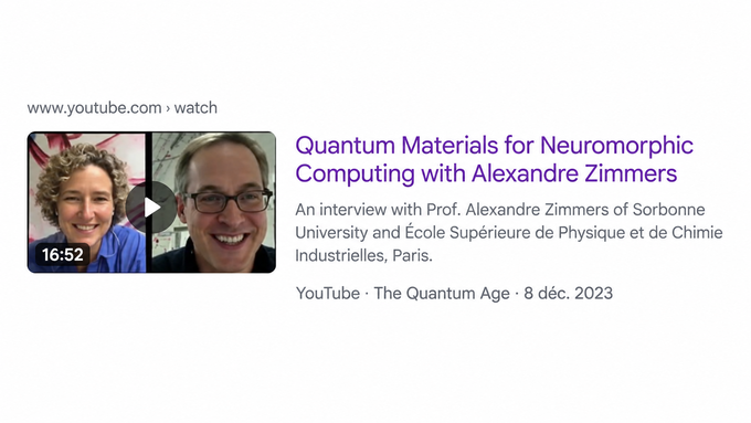
Watch the interview — Quantum Materials for Neuromorphic Computing (16:52)
The Quantum Age — December 2023